Teknik Belgeler
Özellikler
Marka
AlteraArchived Specification Attributes
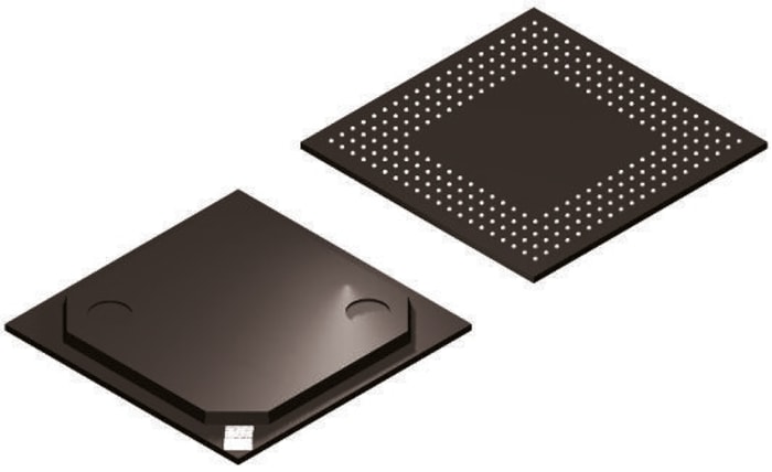
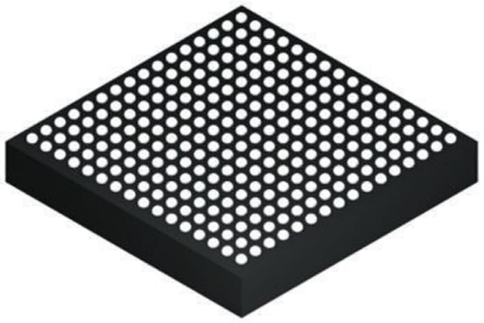
Product Type : FPGA<BR/>Series : 5CEBA2<BR/>Number of Logic Cells : 25000<BR/>Number of Logic Gates : 25000<BR/>Number of RAM Bits : 2002944 bit<BR/>Number of Logic Units : 9434<BR/>Pin Count : 256<BR/>Package Type : FBGA<BR/>Automotive Standard : No<BR/>Length : 17 mm<BR/>Maximum Operating Temperature : 85 °C<BR/>Maximum Supply Voltage : 1.13 V<BR/>Minimum Operating Temperature : 0 °C<BR/>Minimum Supply Voltage : 1.07 V<BR/>Mount Type : Surface<BR/>Number of I/Os : 128<BR/>Number of Multipliers : 50 (18 x 18)<BR/>Number of Registers : 37736<BR/>Standards/Approvals : No<BR/>Width : 17 mm
Ürün Ayrıntıları
An FPGA is a semiconductor device consisting of a matrix of Configurable Logic Blocks (CLBs) connected through programmable interconnects. The user determines these interconnections by programming SRAM. A CLB can be simple (AND, OR gates, etc) or complex (a block of RAM). The FPGA allows changes to be made to a design even after the device is soldered into a PCB.

Ideate. Create. Collaborate
JOIN FOR FREE
No hidden fees!


Stok bilgileri geçici olarak kullanılamıyor.
3.511,20 TL
3.511,20 TL Each (KDV Hariç)
4.213,44 TL
4.213,44 TL Each KDV Dahil
Standart
1
3.511,20 TL
3.511,20 TL Each (KDV Hariç)
4.213,44 TL
4.213,44 TL Each KDV Dahil
Stok bilgileri geçici olarak kullanılamıyor.
Standart
1
Ideate. Create. Collaborate
JOIN FOR FREE
No hidden fees!
Teknik Belgeler
Özellikler
Marka
AlteraArchived Specification Attributes
Product Type : FPGA<BR/>Series : 5CEBA2<BR/>Number of Logic Cells : 25000<BR/>Number of Logic Gates : 25000<BR/>Number of RAM Bits : 2002944 bit<BR/>Number of Logic Units : 9434<BR/>Pin Count : 256<BR/>Package Type : FBGA<BR/>Automotive Standard : No<BR/>Length : 17 mm<BR/>Maximum Operating Temperature : 85 °C<BR/>Maximum Supply Voltage : 1.13 V<BR/>Minimum Operating Temperature : 0 °C<BR/>Minimum Supply Voltage : 1.07 V<BR/>Mount Type : Surface<BR/>Number of I/Os : 128<BR/>Number of Multipliers : 50 (18 x 18)<BR/>Number of Registers : 37736<BR/>Standards/Approvals : No<BR/>Width : 17 mm
Ürün Ayrıntıları
An FPGA is a semiconductor device consisting of a matrix of Configurable Logic Blocks (CLBs) connected through programmable interconnects. The user determines these interconnections by programming SRAM. A CLB can be simple (AND, OR gates, etc) or complex (a block of RAM). The FPGA allows changes to be made to a design even after the device is soldered into a PCB.
Ideate. Create. Collaborate
JOIN FOR FREE
No hidden fees!